- 您现在的位置:买卖IC网 > Sheet目录479 > MRF89XA-I/MQ (Microchip Technology)TXRX ISM SUB-GHZ ULP 32QFN
MRF89XA
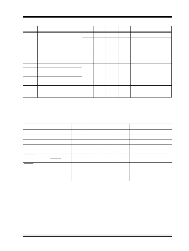
TABLE 5-6:
TRANSMITTER AC CHARACTERISTICS (1)
Symbol
RFOP
Description
RF Output Power, Programmable
with 8 Steps of typ. 3 dB
Min
—
—
Typ
+12.5
-8.5
Max
—
—
Unit
dBm
dBm
Condition
Maximum power setting.
Minimum power setting.
PN
Phase Noise
—
-112
—
dBc/Hz Measured with a 600 kHz
offset at the transmitter output.
TXSP
Transmitted Spurious
—
—
-47
dBc
At any offset between 200 kHz
and 600 kHz, unmodulated
carrier, f dev = 50 kHz.
TX2
Second Harmonic
No modulation, see Note 2
TX3
TX4
Third Harmonic
Fourth Harmonic
—
—
-40
dBm
TXn
Harmonics above TX4
FSKDEV
TSTWF
TSTWS
FSK Deviation
Transmitter Wake-up Time
Transmitter Wake-up Time
±33
—
—
±55
120
600
-200
500
900
kHz
μs
μs
Programmable
From FS to TX ready.
From Stand-by to TX ready.
Note 1:
2:
Guaranteed by design and characterization.
Transmitter in-circuit performance with RFM recommended SAW filter and crystal.
5.2
Timing Specification and Diagram
TABLE 5-7:
SPI TIMING SPECIFICATION (1,2,3)
Parameter
SPI Configure Clock Frequency
SPI Data Clock Frequency
Data Hold and Setup Time
SDI Setup Time for SPI Configure
SDI Setup Time for SPI Data
CSCON Low to SCK Rising Edge;
Min
—
—
2
250
312
500
Typ
—
—
—
—
—
—
Max
6
1
—
—
—
—
Unit
MHz
MHz
μs
ns
ns
ns
Condition
—
—
—
—
—
—
SCK Falling Edge to CSCON High
CSDAT Low to SCK Rising Edge;
625
—
—
ns
—
SCK Falling Edge to CSDAT High
CSCON Rising to Falling Edge
CSDAT Rising to Falling Edge
500
625
—
—
—
—
ns
ns
—
—
Note 1:
2:
Typical Values: T A = 25°C, V DD = 3.3V, crystal frequency = 12.8 MHz, unless otherwise specified.
Negative current is defined as the current sourced by the pin.
? 2010–2011 Microchip Technology Inc.
Preliminary
DS70622C-page 107
发布紧急采购,3分钟左右您将得到回复。
相关PDF资料
MRF89XAM9A-I/RM
IC TXRX MOD 915MHZ ULP SUB-GHZ
MRX-001-433DR-B
MODULE RECEIVER 433MHZ 18DIP
MRX-002-433DR-B
MODULE RECEIVER 433MHZ 18DIP
MRX-002SL-433DR-B
MODULE RCVR 433MHZ SAW LN 24DIP
MRX-005-915DR-B
MODULE RECEIVER 915MHZ 18DIP
MRX-005SL-915DR-B
MODULE RCVR 915MHZ SAW LN 24DIP
MRX-007-433DR-B
MODULE RECEIVER 433MHZ 18DIP
MRX-008-433DR-B
MODULE RECEIVER 433MHZ 18DIP
相关代理商/技术参数
MRF89XAM8A-I
制造商:MICROCHIP 制造商全称:Microchip Technology 功能描述:Ultra Low-Power, Integrated ISM Band Sub-GHz Transceiver
MRF89XAM8A-I/RM
功能描述:射频模块 868MHz Sub-GHz transceiver module
RoHS:否 制造商:Linx Technologies 产品:Transceiver Modules 频带:902 MHz to 928 MHz 输出功率:- 15.5 dBm to + 12.5 dBm 接口类型:UART 工作电源电压:- 0.3 VDC to + 5.5 VDC 传输供电电流:38.1 mA 接收供电电流:22.7 mA 天线连接器类型:U.FL 最大工作温度:+ 85 C 尺寸:1.15 mm x 0.63 mm x 0.131 mm
MRF89XAM8A-I/RM
制造商:Microchip Technology Inc 功能描述:, Leaded Process Compatible:Yes, Peak Re
MRF89XAM9A_12
制造商:MICROCHIP 制造商全称:Microchip Technology 功能描述:915 MHz Ultra Low-Power Sub-GHz Transceiver Module
MRF89XAM9A-I/RM
功能描述:射频模块 915MHz Sub-GHz Transceiver Mod RoHS:否 制造商:Linx Technologies 产品:Transceiver Modules 频带:902 MHz to 928 MHz 输出功率:- 15.5 dBm to + 12.5 dBm 接口类型:UART 工作电源电压:- 0.3 VDC to + 5.5 VDC 传输供电电流:38.1 mA 接收供电电流:22.7 mA 天线连接器类型:U.FL 最大工作温度:+ 85 C 尺寸:1.15 mm x 0.63 mm x 0.131 mm
MRF89XAM9AT-I/RM
制造商:Microchip Technology Inc 功能描述:915 MHz Ultra Low-Power Sub-GHz Transceiver Module
MRF89XAT-I/MQ
功能描述:射频收发器 868/915/950 MHz Sub-GHz transceiver RoHS:否 制造商:Atmel 频率范围:2322 MHz to 2527 MHz 最大数据速率:2000 Kbps 调制格式:OQPSK 输出功率:4 dBm 类型: 工作电源电压:1.8 V to 3.6 V 最大工作温度:+ 85 C 接口类型:SPI 封装 / 箱体:QFN-32 封装:Tray
MRF8HP21080HR3
功能描述:射频MOSFET电源晶体管 HV8 2.1GHZ 160W NI780H-4 RoHS:否 制造商:Freescale Semiconductor 配置:Single 晶体管极性: 频率:1800 MHz to 2000 MHz 增益:27 dB 输出功率:100 W 汲极/源极击穿电压: 漏极连续电流: 闸/源击穿电压: 最大工作温度: 封装 / 箱体:NI-780-4 封装:Tray
